Experimental physics · Semiconductor technology

Dmitry
Shcherbakov, PhD

Experimental physicist specializing in semiconductor devices, nanofabrication, and electrical characterization.

My research combines device fabrication, low-temperature charge-transport measurements, and quantitative data analysis.

St. Louis, Missouri · Open to R&D and semiconductor engineering opportunities

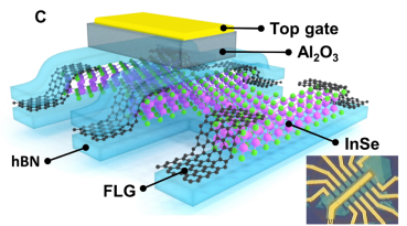
Published schematic of an InSe device: top gate, aluminum oxide, hBN encapsulation, few-layer graphene contacts, and InSe channel, with an optical device image.

InSe device · Figure 1C

Shcherbakov et al., Science Advances (2021).
© The Authors · CC BY-NC 4.0 · Cropped from Figure 1.
Source publication ↗
PhD in Physics · Ohio State10+ years of research experienceFabrication → Measurement → Analysis

Research projects

Four first-author publications · 2018–2024
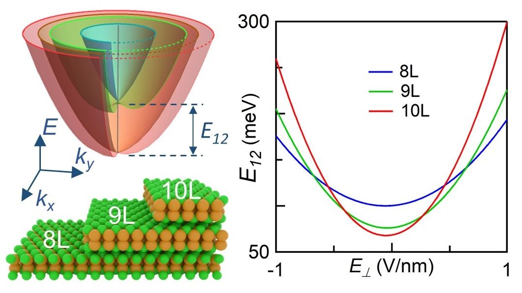
Transport maps, density-of-states simulation, and extracted subband energy-spacing curves from the 2024 InSe study.
Figure 3 · © 2024 American Chemical Society · Cropped from the paper
Nano Letters · 2024 · First author

Electrically tunable InSe quantum wells

Fabricated and measured dual-gated, atomically thin InSe devices to study electrical control of electronic subbands. Transport analysis revealed subband energy-spacing tunability exceeding 350% in a 10-layer device.

Device fabrication · Cryogenic transport · Fourier analysis

Read paper ↗
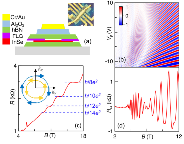
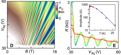
Figure 1: InSe device schematic, optical image, magnetotransport map, and quantum Hall resistance traces.
Figure 1 · © 2022 American Physical Society · Cropped from the paper
Physical Review B · 2022 · First author

Quantum Hall transport in InSe

High-field and temperature-dependent transport measurements resolve quantum Hall states and their energy gaps. The study shows how strong spin-orbit coupling changes the interpretation of effective mass and g-factor extracted from measurements.

Magnetotransport · Thermal activation · Parameter extraction

Read paper ↗
Figure 1D–E: InSe magnetotransport map and temperature-dependent oscillation amplitudes.
Figure 1D–E · © 2021 The Authors · CC BY-NC 4.0 · Cropped from the paper
Science Advances · 2021 · First author

Gate- and layer-tunable spin-orbit coupling

Fabricated and measured few-layer InSe devices, using quantum oscillations and Fourier analysis to characterize spin-orbit coupling. Independent control of carrier density and electric field enabled spin splitting tunable between 0 and 20 meV.

Dual-gated devices · Quantum oscillations · Data analysis

Read paper ↗
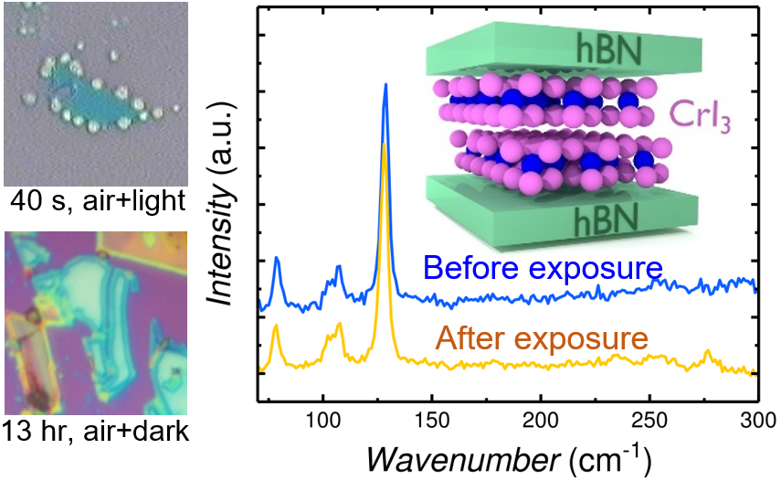
Figure 3: optical images of CrI3 under different protective layers and Raman spectra before and after exposure.
Figure 3 · © 2018 American Chemical Society · Cropped from the paper
Nano Letters · 2018 · First author

Stabilizing air-sensitive CrI₃

Raman spectroscopy, microscopy, and electrical measurements reveal how light and moisture degrade atomically thin CrI₃. Comparing protective layers identified hBN sandwich encapsulation that preserved samples for over 10 days in ambient conditions in the dark.

Raman spectroscopy · Degradation analysis · Encapsulation

Read paper ↗
Technical expertise

Technical skills

My work connects fabrication processes, experimental systems, and the analysis needed to understand device behavior.

Nanofabrication & thin films

Electron-beam lithography, evaporation, sputtering, reactive-ion etching, ion milling, lift-off, and dry and wet transfer of thin films and van der Waals heterostructures.

Electrical characterization & metrology

Charge transport, cryogenic systems, high magnetic fields, lock-in measurements, vacuum systems, SEM, AFM, and Raman spectroscopy.

Scientific computing & data analysis

MATLAB scripts for charge-transport data processing, alongside experience with Igor Pro, Python, and Mathematica. Turning measured signals into interpretable plots and physical parameters.

Measurements→Processing→Physical insight
Background

Research experience

Experience developing nanoscale electronic devices, troubleshooting fabrication and measurement challenges, and communicating results through scientific publications.

PhD in Physics · 2021
The Ohio State University

MS & BS in Applied Mathematics and Physics
Moscow Institute of Physics and Technology

Washington University in St. Louis

Postdoctoral Associate · 2D materials, thin-film heterostructures, device fabrication, and electrical characterization.

Carnegie Mellon University

Postdoctoral Associate · Ultrathin field-effect transistors, twisted graphene, and graphene–semiconductor interfaces.

The Ohio State University

Research and Teaching Assistant · Charge transport in 2D materials and semiconductor devices.

University of California, Riverside

Research and Teaching Assistant · Ultrathin field-effect transistor fabrication.

Download my full CV ↓
Let’s connect

Contact

I’m interested in R&D, process, materials, and equipment engineering roles in semiconductor technology.

Email Dmitry ↗